
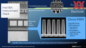
Intel is poised to redefine chiplet technology with its 18A process,enabling breakthroughs in performance and power efficiency for upcoming processors like Panther Lake and Clearwater Forest. unveiled during the Intel ITT US event,the 18A process leverages PowerVia,RibbonFET,and advanced Foveros packaging to overcome longstanding scaling challenges and deliver a significant leap forward in semiconductor manufacturing.
The advancements detailed represent a critical inflection point for Intel as it aims to regain process technology leadership and capitalize on the growing demand for heterogeneous computing. These innovations will impact a broad range of users, from consumers seeking higher performance in PCs to data centers requiring increased computational density and reduced energy consumption. Intel’s success with 18A will determine its competitive position against rivals like TSMC and Samsung, and influence the future trajectory of the semiconductor industry.
Foveros-S, utilizing a bump pitch of 36 µm or less-with Foveros-R and Foveros-B variants expected at 25 µm-allows for silicon interposers four times the size of current reticle limits, establishing it as a core packaging technology at Intel. Clearwater Forest will integrate both Embedded Multi-Die Interconnect Bridge (EMIB),already in mass production since 2019 and first used in Kaby Lake-G with an AMD GPU,and foveros Direct 3D.
Foveros Direct 3D is a key differentiator for Clearwater Forest,featuring a 9 µm bump pitch,hybrid bonding with copper-to-copper connections,and exceptionally efficient data transmission at 50 nJ/bit. Historically, Intel’s packaging capabilities have primarily served its internal product divisions, but the company is actively seeking external customers, promoting its advanced packaging services alongside chip and wafer testing.
The data in this article was obtained by Hardwareluxx during Intel’s invitation to the Intel Tech Tour US in Phoenix, Arizona, with travel and accommodation costs covered by Intel.