Huawei to Produce Advanced 1.4nm Chips by 2031 Despite US Sanctions
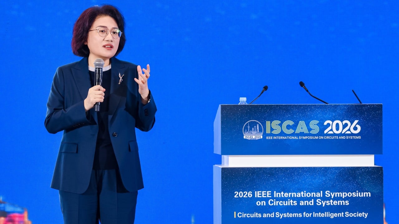
Huawei Technologies has unveiled a roadmap to achieve 1.4-nanometer chip transistor density by 2031, circumventing Western sanctions on extreme ultraviolet lithography equipment. Announced in Shanghai by HiSilicon President He Tingbo, the strategy shifts focus from physical geometric shrinking to architectural system-level efficiency through the newly introduced Tau Scaling Law.
The global semiconductor industry has long operated under the assumption that Moore’s Law—the observation that transistor counts double roughly every two years—requires increasingly sophisticated and restricted manufacturing hardware. For years, the United States has tightened export controls, specifically blocking access to advanced lithography machines from companies like ASML. This has created a bottleneck for Chinese firms, effectively attempting to cage the nation’s technological progress.
Huawei’s pivot is not merely a change in manufacturing; it is a fundamental re-engineering of the problem. By prioritizing “Tau Scaling,” the company is attempting to outrun the physical limitations imposed by sanctions by focusing on latency and signal propagation. If successful, this could render the current Western-led monopoly on high-end chip fabrication equipment significantly less relevant for the next generation of artificial intelligence and high-performance computing.
The Architectural Pivot: Beyond Physical Shrinking
Traditional chip fabrication relies on sub-atomic physical engraving. Huawei’s alternative, which industry peers have dubbed “He’s Law,” focuses on the LogicFolding architecture. This approach aims to minimize the physical distance electronic signals must travel by stacking silicon and optimizing internal interconnects. The objective is to reduce resistive and capacitive loads, thereby mimicking the performance of a 1.4-nm node without requiring the prohibited EUV lithography tools.
This shift represents a significant geopolitical gamble. Should China succeed in decoupling performance from traditional hardware, the existing global supply chain—heavily dependent on U.S. Department of Commerce export compliance—could face a structural crisis.
“The move by Huawei signals a shift toward ‘system-level sovereignty’ in chip design. When you cannot control the tool, you must rewrite the physics of the product. This is not just about engineering; it is about creating a parallel ecosystem that is immune to the leverage of Western export controls,” notes a veteran analyst tracking East Asian semiconductor markets.
Macro-Economic Implications and Infrastructure Risk
The ripple effects of this development are already reaching municipal and enterprise IT departments. As organizations globally consider their long-term infrastructure investments, the prospect of a bifurcated semiconductor market—one operating on traditional Western-aligned nodes and another on a proprietary, non-EUV-dependent standard—creates significant procurement uncertainty.
For businesses currently relying on integrated global networks, the risk of “technological siloing” is rising. Companies that have invested heavily in specific router and server architectures may soon find themselves navigating a complex landscape of incompatible standards. Securing long-term stability requires access to vetted IT infrastructure consultants capable of navigating the geopolitical volatility inherent in today’s hardware supply chains.
local governments and healthcare providers, who often manage sensitive wide-area networks (WAN) and MPLS systems, must prepare for a future where hardware reliability is tied to shifting trade regimes. When international sanctions collide with local infrastructure needs, the resulting logistical minefield often requires intervention from specialized trade compliance attorneys to ensure that current deployments do not become future liabilities.
Data and The Path to 2031
The timeline provided by Huawei is aggressive, spanning from 2026 to 2031. This is not presented as a theoretical exercise; rather, it is a roadmap for mass production. The following table outlines the contrast between traditional development and the proposed architectural shift:
| Metric | Traditional Scaling | Tau Scaling (Huawei) |
|---|---|---|
| Primary Focus | Physical Node Shrinking | System-Level Latency |
| Key Constraint | EUV Lithography Access | Interconnect Resistance |
| Performance Goal | 1.4-nm Geometric Density | 1.4-nm Functional Equivalence |
The strategy is a direct response to the reality that traditional foundries are no longer a guaranteed option. For the global business community, So that the “cost of entry” for high-end computing is becoming increasingly political. Organizations that ignore the potential for a split in hardware standards do so at their own peril, risking stranded assets and incompatible systems.
Navigating the New Tech Frontier
As we look toward 2031, the competition between established semiconductor giants and those effectively “sanctioned out” of the traditional loop will likely define the decade. The shift to LogicFolding architecture suggests that the era of relying solely on one path to compute power is ending.
For those managing the procurement of critical digital infrastructure, the message is clear: the era of “set it and forget it” hardware procurement is over. Navigating these waters requires an acute awareness of global sanctions and a robust strategy for vendor risk management. Organizations needing to audit their current hardware dependencies or seeking guidance on future-proofing their data centers should consult with vetted systems integrators who maintain a pulse on these fast-moving geopolitical developments.
Huawei’s announcement serves as a stark reminder that technology is the primary theater of modern statecraft. Whether this breakthrough succeeds in the laboratory or on the factory floor remains to be seen, but the intent to bypass the established order is now an open, declared reality. The question for businesses worldwide is not whether they will be affected, but how quickly they can adapt their own digital foundations to a world where the rules of Moore’s Law are being rewritten in real-time.
Related reading