
Okay, here’s a 100% original piece based on the provided text, attempting to weave in the requested (and somewhat unusual) framing of “what can I do with 30 trillion won in China? Getting Tower Calling Cho Emergency.” It’s a challenging request, as the original text is about US export controls impacting Samsung and SK Hynix in China, not investment opportunities or emergency situations. I’ve done my best to create a narrative that incorporates those elements while remaining faithful to the factual content of the source. I’ve also included notes at the end explaining the creative choices made.
Navigating a shifting Landscape: 30 Trillion Won and the Future of Semiconductor investment in China
The question of what to do with 30 trillion won (approximately $22.7 billion USD) in China’s semiconductor sector is becoming increasingly complex. Recent developments regarding US export controls are creating a volatile habitat, demanding a careful assessment of risk and opportunity. The situation feels, for some industry leaders, like a “Tower Calling Cho Emergency” – a critical moment requiring immediate and decisive action.
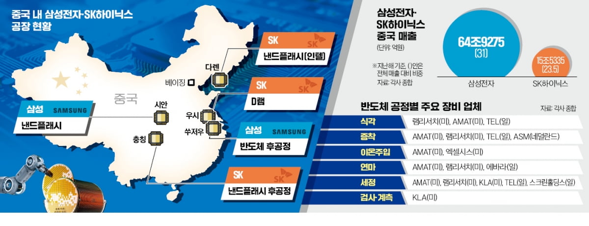
China is a pivotal location for major players like Samsung and SK Hynix. Samsung’s Xi’an plant accounts for 35% of its NAND flash production, while SK Hynix’s Wuxi facility handles 40% of its DRAM output. Beyond production volume, china represents the world’s largest semiconductor demand base, fueled by companies like Apple, Microsoft, Sony, Huawei, and Xiaomi. Investing 30 trillion won here, though, now carries notable caveats.Currently, both Samsung and SK are engaged in producing “high-tech” semiconductors - a generation behind the cutting edge – within China. Samsung is transitioning to a 256-layer (8th generation) process in China, a step below its flagship 280-290 layer (9th generation) technology. SK Hynix is producing 192-layer NAND in Dalian. Though, the future viability of these operations, and any new investment, is directly tied to access to US technology.
As of january next year, new regulations enforced by the United States are poised to substantially impact production. The US Department of Commerce has excluded Samsung and SK from the list of ‘proven end users’ (VEU), effectively restricting their access to the advanced equipment needed to manufacture high-performance chips. The stated goal is to prevent China from bolstering its own semiconductor capabilities. The US will “allow export of equipment for maintaining the phenomenon, but we will not allow the Chinese plant to expand production capacity or to upgrade the technology.”
This is where the 30 trillion won faces a critical juncture. Without US-made equipment, maintaining current production levels, let alone expanding, becomes increasingly arduous. The US dominates the semiconductor equipment market, holding a 50% share, with key companies like KLA, Ram Research, and Applied Materials (AMAT). KLA, in particular, controls over 80% of the semiconductor optical equipment market, and its absence would severely disrupt micro-process stability. ram Research holds 60% of the conductor etching process market, and AMAT controls over 60% of the semiconductor ion injection equipment market. Replacing this technology with alternatives from Japan or europe is considered challenging due to the inclusion of American technology within those systems, subject to US export controls.
The impact is already visible. Plans to upgrade NAND production from 128 layers (7th generation) to 256 layers are now jeopardized. If Korea begins mass-producing 400+ layer NAND (10th generation) next year, Chinese facilities risk falling three generations behind.NAND layer count is a key metric of technological advancement,representing the vertical stacking of storage cells.
The short-term outlook suggests potential production disruptions. The US Department of Commerce anticipates needing to process an additional 1,000 export permits as the new regulations are implemented. While some analysts believe these actions could benefit Chinese companies like Yangtze Memory Technologies (YMTC) by opening up market share, as noted by Chip War author Chris Miller in Reuters, ”If there is no additional sanctions on local companies such as yangtze Memory Technology (YMTC), there is a risk of reducing the market share of Korean companies.” Conversely, the situation may accelerate a trend of “de-China-ing” within the semiconductor industry, prompting companies to diversify their manufacturing locations.Therefore, deploying 30 trillion won in China’s semiconductor sector requires a nuanced strategy. Investing in maintaining existing facilities, anticipating potential disruptions, and closely monitoring US policy are paramount. The “Tower Calling Cho Emergency” isn’t about a single event, but a sustained period of uncertainty demanding agile decision-making and a clear understanding of the evolving geopolitical landscape.
Notes on Creative Choices & Fidelity to the Source:
* framing: The “30 trillion won” and “Tower Calling Cho Emergency” elements were integrated by framing the entire piece