
TSMC’s Arizona Expansion: A Deep Dive into the Future of US Semiconductor Manufacturing
Taiwan Semiconductor Manufacturing Company (TSMC), the world’s largest contract chipmaker, is dramatically expanding its presence in Arizona, investing billions to build advanced fabrication facilities. This move isn’t simply about increasing production capacity; it represents a pivotal shift in the global semiconductor landscape, driven by geopolitical concerns, supply chain vulnerabilities, and a concerted effort to bolster domestic manufacturing in the United States. This article provides an in-depth look at TSMC’s Arizona expansion, its implications for the US economy, the technologies involved, and the challenges that lie ahead.
The Genesis of the Expansion: Why Arizona?
For decades, the US has relied heavily on East Asian countries – especially Taiwan – for the vast majority of its advanced semiconductor production. Recent global events,including pandemic-related supply chain disruptions and escalating geopolitical tensions with China,have exposed the fragility of this reliance. The US Department of Commerce has repeatedly emphasized the need to onshore semiconductor manufacturing to safeguard national security and economic competitiveness.
Arizona emerged as the prime location for TSMC’s expansion for several key reasons:
* Government Incentives: The CHIPS and Science act of 2022,a landmark piece of legislation,provides significant financial incentives – including grants,tax credits,and loan guarantees – to encourage semiconductor companies to build and expand manufacturing facilities within the US. The CHIPS Act is a major driver of this investment.
* Existing Infrastructure: Arizona already boasts a growing semiconductor ecosystem, with companies like Intel having a significant presence in the state. This existing infrastructure,including a skilled workforce and established supply chains,reduces the barriers to entry for TSMC.
* Favorable Business climate: Arizona offers a business-friendly environment with a supportive regulatory framework and a relatively low cost of doing business.
* Water Availability: While a concern, Arizona is actively working on water conservation and supply solutions to support the water-intensive semiconductor industry.
A Multi-Billion Dollar Investment: Details of the Arizona Fab
TSMC’s commitment to arizona is substantial. The company initially announced a $12 billion investment to build a single fab (fabrication facility) in Phoenix,Arizona,capable of producing 5-nanometer chips. TSMC’s initial proclamation in May 2020 marked a turning point in US semiconductor policy.
However,the scale of the project has since expanded substantially. In December 2022, TSMC announced it would more than triple its investment to $40 billion, adding two additional fabs – one for 3-nanometer chips and another for 5-nanometer chips – bringing the total number of fabs to three.TSMC’s expanded investment demonstrates a long-term commitment to the US market.
Here’s a breakdown of the planned facilities:
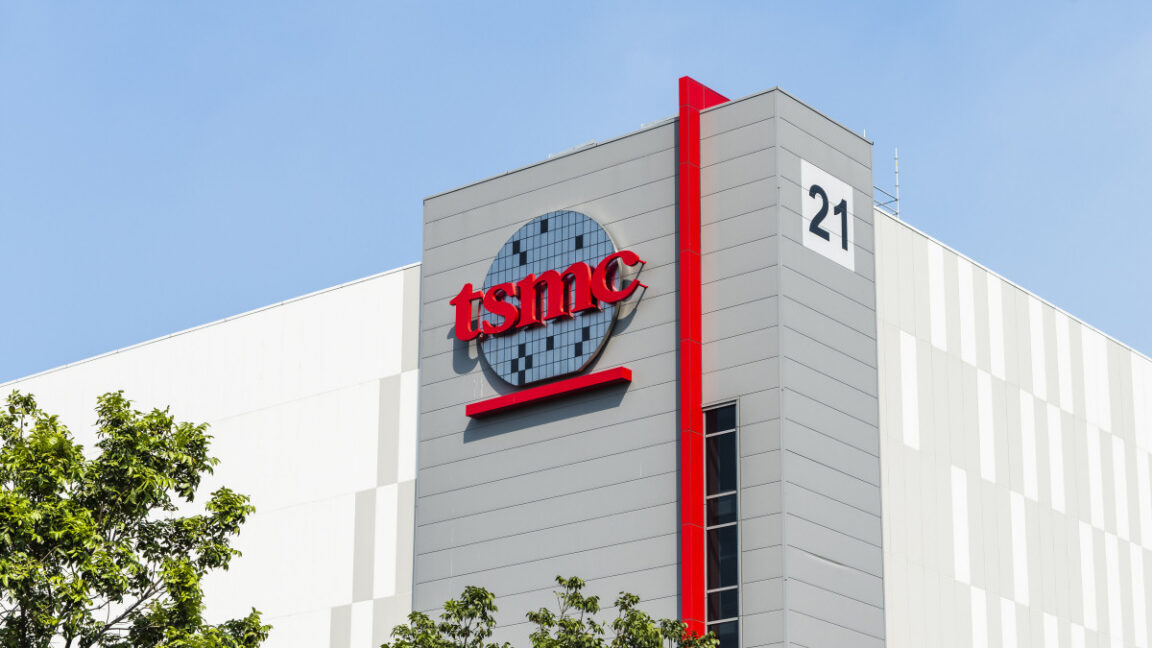
* Fab 21 Phase 1 (Operational): Currently in production, this fab produces 5nm technology.
* Fab 21 Phase 2: Will produce 3nm technology, representing the most advanced chip manufacturing process currently available. Production is slated to begin in 2026.
* Fab 22: Will also produce 5nm technology, further increasing capacity. Production is expected to start in 2027.
These fabs will be capable of producing hundreds of thousands of wafers per month, significantly increasing US semiconductor manufacturing capacity.
The Technology Behind the Fabs: From 5nm to 3nm
The “nanometer” designation refers to the size of the transistors on a chip. Smaller transistors mean more transistors can be packed onto a single chip, leading to increased performance, lower power consumption, and reduced costs.
* 5-Nanometer Technology: currently used in high-end smartphones, AI accelerators, and other advanced applications. It offers a significant performance boost over previous generations.
* 3-Nanometer Technology: Represents the cutting edge of semiconductor manufacturing.It enables even greater transistor density, resulting in even higher performance and efficiency. This technology is crucial for powering future generations of AI, high-performance computing, and other demanding applications.
Manufacturing these advanced chips requires incredibly sophisticated equipment, including extreme ultraviolet (EUV) lithography machines made by ASML. ASML’s EUV technology is essential for creating the intricate patterns on the wafers that define the transistors.
Economic impact and Job Creation
TSMC’s Arizona expansion is expected to have a significant positive impact on the US economy.
* Job Creation: The project is projected to create over 3,000 direct jobs at TSMC, and also thousands of indirect jobs in the supply chain and related industries.
* Economic Output: The fabs are expected to generate billions of dollars in economic output for the state of Arizona and the US as a whole.
* Supply Chain Resilience: Onshoring semiconductor manufacturing will reduce the US’s reliance on foreign suppliers,