
Altering Heat Transport at the Chip Component Level – Summary
This article details a new method for controlling heat dissipation in microchips using ultrafast laser pulses to create nanoscale grooves on the chip surface. HereS a breakdown of the key points:
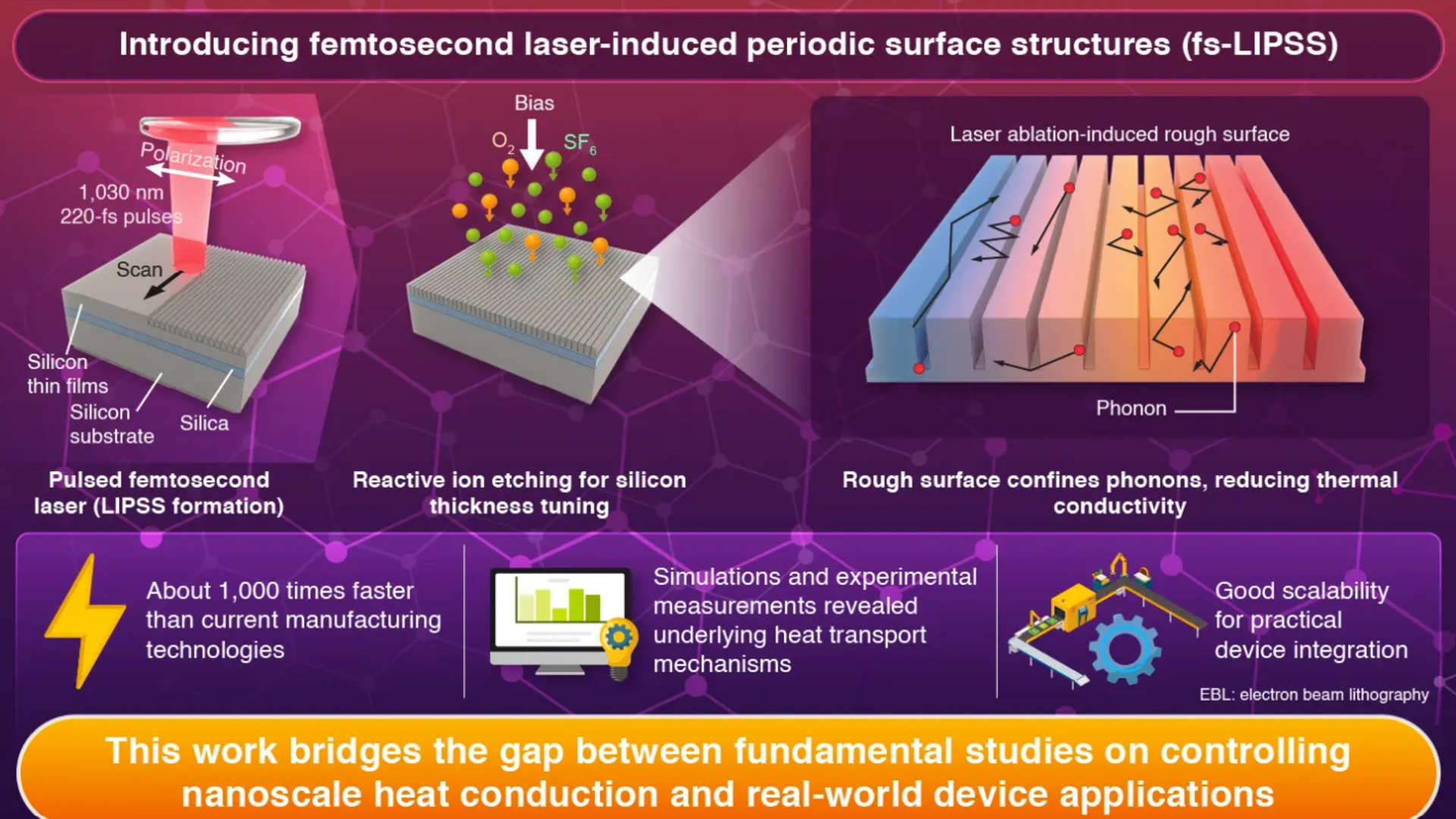
* How it works: Femtosecond laser pulses ablate material, creating precisely spaced and deep grooves that disrupt the travel of phonons (the primary heat carriers in these components).
* Result: This disruption reduces thermal conductivity in a predictable way. The patterned surfaces, called femtosecond laser-induced periodic surface structures (fs-LIPSS), are uniform over large areas. Combining this with dry etching for thickness adjustment further enhances the reduction.
* Verification: The reduction in thermal conductivity was confirmed through thermoreflectance measurements and numerical simulations, showing it’s due to limited phonon travel, not material changes.
* Advantages:
* Speed: Over 1000x faster than electron-beam lithography.
* Efficiency: Maskless and resist-free, simplifying the process.
* Scalability: Suitable for wafer-scale implementation and integration with existing CMOS manufacturing.
* Compatibility: Doesn’t require additional components or lithographic steps and works with established semiconductor workflows.
* Applications: Notably useful for thermal layers in high-performance applications like data center processors.
In essence,this technique offers a fast,efficient,and scalable way to manage heat in microchips,possibly leading to more powerful and reliable electronic devices.