Huawei’s Breakthrough Chip Tech: How 3D Innovation Could Reshape the Semiconductor War
Huawei Technologies Co. Ltd. has unveiled a proprietary 3D chip architecture designed to circumvent Western export restrictions, aiming to close the performance gap with industry leaders like TSMC. Following a reported $127 million in revenue growth despite stringent U.S. sanctions, this technological pivot signals a high-stakes shift in China’s domestic semiconductor independence strategy.
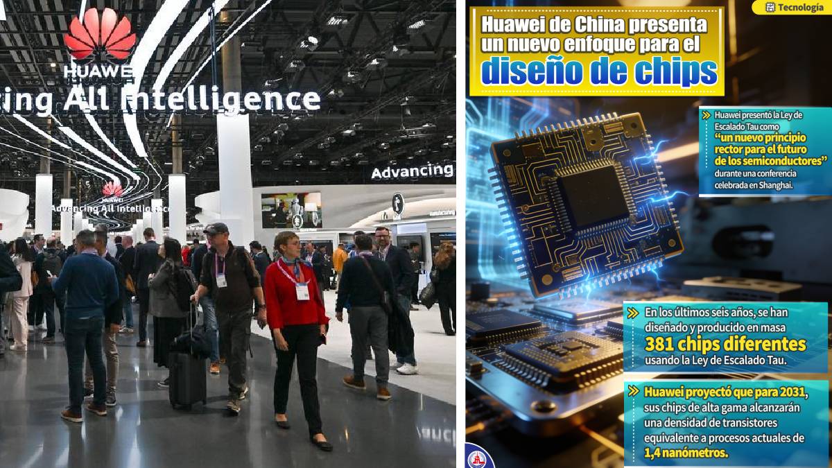
The Technical Pivot: Beyond Conventional Lithography
Huawei’s latest design methodology focuses on 3D stacking and advanced packaging, techniques that allow for increased transistor density without requiring the extreme ultraviolet (EUV) lithography machines currently barred from export to China. By re-engineering the physical layout of the silicon die, the firm seeks to maintain competitive power-efficiency profiles in its high-end Kirin processors.
This development is not merely an engineering feat; it is a response to the severe supply chain constraints identified in the latest Huawei Annual Report. The company has been forced to pivot away from traditional node-shrinking processes, which rely on access to Dutch-made ASML machinery, toward architectural ingenuity. For hardware manufacturers and data center operators, this shift introduces a new layer of volatility in hardware lifecycle management. Organizations facing hardware compatibility risks often engage specialized semiconductor supply chain risk management firms to audit their long-term infrastructure dependencies.
Fiscal Realities and the $127M Revenue Delta
The financial narrative surrounding Huawei in 2026 is defined by a paradox: restricted access to global markets and a surge in domestic demand. Recent filings indicate that despite being blacklisted by the U.S. Bureau of Industry and Security, the firm generated $127 million in revenue during the most recent measurement period. This indicates a robust internal market willing to pay a premium for “sovereign” tech.
However, the cost of innovation remains high. Research and development expenditures have ballooned as the firm attempts to domesticate the entire semiconductor stack. “The transition from importing off-the-shelf high-end silicon to building a vertically integrated, proprietary ecosystem is capital-intensive and fraught with yield-rate inefficiencies,” notes Marcus Thorne, a senior technology strategist at Global Equity Research. “Investors should watch for sustained pressure on EBITDA margins as these R&D costs hit the balance sheet throughout the next three fiscal quarters.”
Comparative Performance Metrics
The following table outlines the current competitive positioning based on public financial disclosures and industry-standard performance benchmarks:

| Metric | Huawei (Projected) | TSMC (Industry Standard) |
|---|---|---|
| Lithography Reliance | Deep Ultraviolet (DUV) + 3D Stacking | EUV + Advanced Packaging |
| Revenue Growth Trend | High Domestic/Low Global | High Global Diversification |
| Capex Intensity | High (Systemic Rebuild) | Moderate (Maintenance/Expansion) |
Managing the Domestic “Chip War”
While the international narrative focuses on the U.S.-China trade war, internal industry reports highlight a more nuanced competition. Domestic Chinese firms are struggling to maintain parity with Huawei’s government-backed R&D pace. This creates a secondary market problem: smaller tech firms are being squeezed out of the supply chain as Huawei consolidates access to the limited pool of domestic talent and raw materials.
This market consolidation creates significant legal and regulatory friction. Companies attempting to navigate these shifting trade waters often require international trade law and compliance advisory services to ensure their procurement strategies do not inadvertently trigger secondary sanction risks. As the industry approaches Q4 2026, the cost of non-compliance—ranging from asset freezing to total market exclusion—is rising sharply.
Market Trajectory and Future Outlook
The success of Huawei’s 3D chip strategy hinges on yield stability. If their manufacturing processes fail to achieve the 90%+ yield rates common at TSMC, the cost-per-unit will remain unsustainable for mass-market adoption. Markets are currently pricing in a period of “controlled stagnation,” where the company manages to survive through state support but fails to achieve the economies of scale necessary to challenge global leaders in cost-efficiency.
Investors and procurement officers should prepare for a bifurcated semiconductor market. The era of a singular, globally standardized chip architecture is effectively ending. Firms that fail to diversify their hardware procurement strategy or ignore the geopolitical risks inherent in their supply chain are increasingly vulnerable. For those needing to restructure their procurement or mitigate legal exposure, exploring the vetted expertise found in the World Today News Directory remains the most viable path toward securing long-term operational continuity.