Glass Substrates Face Commercial Delays Amid Industry Roadmap Shifts
Glass Substrate Roadmaps Examined: Absolics in Final Qualification and First Products Facing Slip Timelines
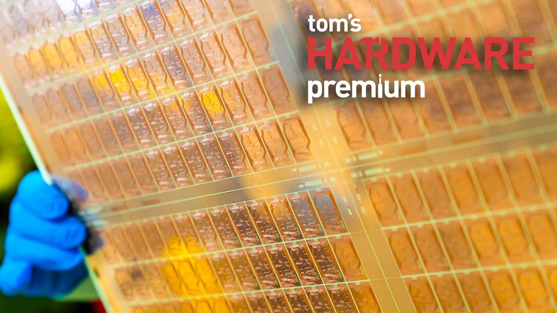
Glass-core substrates, the critical packaging replacement for organic chip substrates backed by more than $1 billion from Intel since September 2023, have officially reached final qualification stages while remaining absent from any commercial product line. According to SKC’s July 27 earnings call, embedded glass substrate samples originating from the Absolics facility in Covington, Georgia, are currently undergoing package-level reliability evaluations in Taiwan, with performance readouts expected before year-end. On July 2, Samsung Electro-Mechanics and Sumitomo Chemical’s Dongwoo Fine-Chem officially established a glass-core joint venture valued at 482.1 billion won ($310 million), with the goal of commencing initial production in the second half of 2027. Intel has pivoted toward licensing its foundational patents and demonstrating reference vehicles, pushing its own commercial deployment out toward 2030. Every historical timeline in the high-density packaging segment has slipped, with Absolics having originally targeted mass production for the first half of 2024.
The Tech TL;DR:
- Supply Chain Bottlenecks: While Absolics and Samsung race toward 2026 and 2027 manufacturing targets, major consumer demand-side players like AMD, Apple, and AWS continue slow qualification cycles or extend evaluation schedules.
- Architectural Gains: Glass cores offer up to 10 times the interconnect density of organic substrates, a 50% reduction in pattern distortion, and tighter thermal expansion matching silicon.
-
Production Realities: Edge-cracking challenges during drilling and dicing remain partially mitigated by modern edge-coating techniques, but nanometer-scale flatness over large panels remains a live engineering problem.
The Thermal and Physical Case for Glass-Core Substrates
The technical impetus for moving away from traditional organic ABF (Ajinomoto Build-up Film) substrates relies on hard numbers published in Intel technical documentation. Glass cores deliver roughly 10 times the interconnect density of standard organic packages alongside a 50% reduction in pattern distortion. Thermal expansion coefficients can be precisely tuned to a range of 3 to 10 ppm per degree Celsius against silicon’s 2.6 ppm/°C, cutting warpage by approximately half compared to organic alternatives. Furthermore, rectangular panels sized at an emerging 510mm x 515mm format yield more than 75% usable area for large die processing, a sharp improvement over the roughly 50% efficiency harvested from round 300mm silicon wafers. Through-glass vias (TGVs) have been successfully demonstrated down to six microns in diameter with aspect ratios exceeding 15:1 at ECTC 2025, while Georgia Tech research displays stacked glass running smoothly at 220 GHz with a minimal 0.3 dB of signal loss.
Yet, physics introduces steep manufacturing penalties. Glass is inherently brittle, causing plates to chip and crack at the edges during high-speed drilling and dicing. Early testing runs at Absolics experienced high failure rates, breaking hundreds of panels every couple of days, as reported by MIT Technology Review in March. While subsequent edge-coating applications successfully dropped measured edge stress from 95 MPa down to 49 MPa, and low-temperature dielectrics curing below 180°C were introduced to minimize thermal stress during build-up layers, metallizing vias under 10 microns and holding strict nanometer-scale flatness across half-meter panels remain active manufacturing hurdles.
# Calculate TGV density and aspect ratio thresholds for panel-level packaging
python3 -c '
diameter_um = 6.0
depth_um = 90.0  # 15:1 aspect ratio target
aspect_ratio = depth_um / diameter_um
print(f"Target TGV Diameter: {diameter_um} um")
print(f"Calculated Aspect Ratio: {aspect_ratio}:1")
if aspect_ratio >= 15.0:
    print("Status: Meets ECTC 2025 high-density specs")
else:
    print("Status: Fails aspect ratio threshold")
'
Absolics, Samsung, and the Global Manufacturing Footprint
Absolics’ $600 million manufacturing facility in Covington, Georgia—bolstered by $75 million in direct U.S. CHIPS Act funding and an additional $100 million through an advanced packaging R&D program with Georgia Tech—maintains a Phase 1 operational capacity of 12,000 square meters of substrate per year. This output volume translates to roughly two to three million H100-sized packages. According to trade reporting from The Elec, Absolics produced early mass-production samples in the first quarter, pushing customer qualification loops that encompass firms like AMD and AWS, with commercial mass production officially targeted by the end of 2026. However, industry analysts note that initial order volumes from anchor customers may lag behind total fab capacity until server-side adoption reaches scale.
In South Korea, Samsung Electro-Mechanics elevated its internal glass program from advanced R&D into a dedicated business-execution unit, running pilot samples out of its Sejong plant since late 2024. The GLASEM joint venture established on July 2 splits equity 66% to Samsung Electro-Mechanics and 34% to Dongwoo Fine-Chem, anchoring its production site in Pyeongtaek to supply drilled and metallized glass cores directly into Samsung’s advanced packaging line. Korean industry tracking notes that sample shipments have reached AMD and Broadcom, though overall process maturity sits at approximately 40 out of 100, underscoring the gap between aggressive marketing schedules and fab floor execution. Meanwhile, LG Innotek is advancing its own program from Gumi, targeting production between 2027 and 2028 following prototype deliveries in 2024.
Enterprises evaluating these next-generation packaging roadmaps must carefully audit their hardware supply chains.
Intel Foundry, TSMC, and Foundry-Level Timelines
Intel demonstrated a working prototype system booting Windows on a glass-core substrate in early 2025. Rahul Manepalli, who serves as Intel’s vice president of module engineering, shared with MIT Technology Review that the advantages provided by glass cores are indisputable. However, the commercial execution plan has evolved. DigiTimes reported that Intel engaged in early-stage discussions with Chinese cover-glass manufacturer Lens Technology regarding a packaging partnership, though no definitive agreement has been finalized.
At NEPCON Japan in January, Intel Foundry displayed its primary thick-core glass substrate housing two EMIB bridge dies embedded straight into the glass: a 78mm x 77mm package incorporating two 800-micron-class glass layers, 10 redistribution layers on each side, and approximately 1,716 square meters of active silicon atop the substrate. TrendForce pegs Intel’s full commercialization timeline around 2030, alongside co-packaged optics prototypes developed at its Rio Rancho, New Mexico facility. Amkor, acting as Intel’s packaging partner on the optics initiative, places commercial readiness within a three-year window based on statements made in Seoul.
Conversely, TSMC’s CoPoS packaging line in Chiayi—built around 310mm x 310mm rectangular panels—received tool installations in February, completed its pilot line setup by June, and targets pilot production by 2027 with volume mass production slated for the second half of 2028. Equipment supplier SCHMID characterizes glass integration within TSMC’s manufacturing lines as currently under review rather than formally committed. TrendForce estimates TSMC’s commercial-scale glass substrate production will likely slide past 2030, indicating that the foundry giant prioritizes panel-level organic packaging before committing to glass cores.
Japanese material suppliers are building concurrent capacity.
FAQ
- Why are glass substrates replacing organic ABF substrates in advanced AI chip packaging?
- Organic substrates experience severe warpage, dimensional instability, and high signal loss as AI accelerator package sizes scale into multiple reticles. Glass cores provide up to 10 times the interconnect density, eliminate significant warpage through tuned thermal expansion coefficients matching silicon, and offer superior surface flatness for multi-die heterogeneous integration.
- When will commercial glass-core substrate packages actually ship to enterprise customers?
- While material suppliers like Absolics and Samsung Electro-Mechanics are targeting customer qualification completions and pilot production runs between late 2026 and 2027, major foundries like Intel and TSMC place broad commercial-scale deployment toward the end of the decade, around 2030.
Disclaimer: The technical analyses and security protocols detailed in this article are for informational purposes only. Always consult with certified IT and cybersecurity professionals before altering enterprise networks or handling sensitive data.