
Cornell University researchers have, for the first time, directly visualized atomic-level defects within functioning computer chips, a breakthrough that could reshape the development and debugging of modern electronics. The new imaging method, detailed in a study published February 23 in Nature Communications, was developed in collaboration with Taiwan Semiconductor Manufacturing Company (TSMC) and Advanced Semiconductor Materials (ASM).
The research centers on identifying imperfections in the transistor channels – the microscopic pathways through which electrical current flows. These defects, even at the scale of a few atoms, can significantly degrade chip performance. “Since there’s really no other way you can spot the atomic structure of these defects, Here’s going to be a really crucial characterization tool for debugging and fault-finding in computer chips, especially at the development stage,” said David Muller, the Samuel B. Eckert Professor of Engineering in the Cornell Duffield College of Engineering, who led the project.
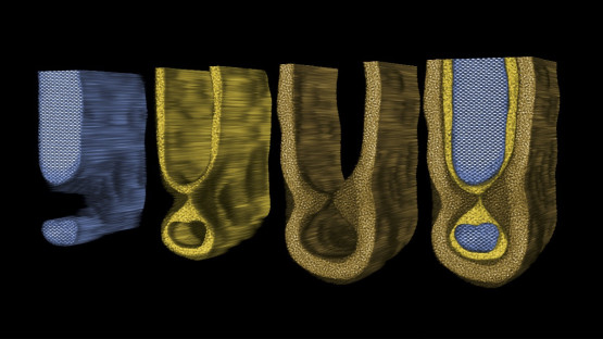
As semiconductor technology continues to shrink, with components now measured in just a few nanometers, identifying and correcting these defects has become increasingly critical. According to the study, the team detected “mouse bites” – a term used to describe roughness at the interfaces within the transistor channels. These imperfections arise during the complex manufacturing process, which involves hundreds, even thousands, of steps of chemical etching, deposition, and heating.
The imaging technique relies on electron ptychography, a computational method utilizing an electron microscope pixel array detector (EMPAD) co-developed by Muller’s group. This technology collects detailed scattering patterns of electrons as they pass through the transistors. By analyzing changes in these patterns, scientists can reconstruct extraordinarily high-resolution images. The detector’s precision has been recognized by Guinness World Records for achieving the highest resolution images of atoms to date.
Muller’s involvement in semiconductor design dates back to his time at Bell Labs from 1997 to 2003, where he explored the physical limits of transistor miniaturization. During his tenure at Bell Labs, Muller and scientist Glen Wilk, now vice president of technology at ASM, investigated replacing silicon dioxide – a common gate material prone to current leakage at smaller scales – with hafnium oxide. This research ultimately led to hafnium oxide becoming the industry standard for computer and cell phone manufacturing in the mid-2000s.
“The papers we published on how to use electron microscopes to characterize these materials, I can advise you, a lot of the semiconductor folks had read those particularly, very carefully,” Muller said. The current collaboration with TSMC and ASM represents a return to this earlier work, leveraging significantly advanced microscopy capabilities. “Back then, it was like flying biplanes. And now you’ve got jets.”
The ability to visualize these defects with atomic precision offers a new level of control over the manufacturing process. “Before you used to glance at projective images to try to figure out what was really going on. Now you have a direct probe to actually see after every single step and have a better grasp of, oh, I position the temperature this high, and then this is what it looks like,” explained doctoral student Shake Karapetyan, the lead author of the study.
The implications of this research extend beyond conventional computing. The researchers suggest the technique could be invaluable for debugging next-generation technologies, including quantum computers, which demand even more precise structural control of materials. The research was funded by TSMC, with support for the microscopy facilities provided by the National Science Foundation-funded Cornell Center for Materials Research (CCMR) and Platform for the Accelerated Realization, Analysis and Discovery of Interface Materials (PARADIM).