
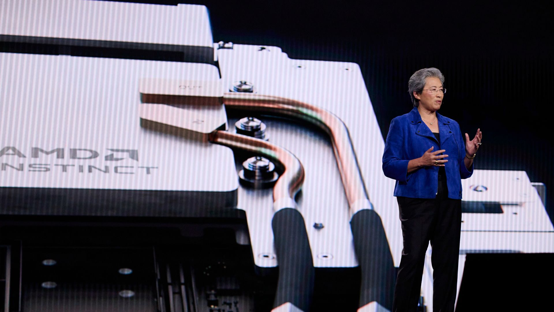
AMD detailed significant engineering advancements within its Instinct MI355X AI accelerator at the ISSCC symposium in San Francisco on February 16, revealing how the company doubled compute throughput while maintaining a similar die area to its predecessor. The MI355X, based on the CDNA 4 architecture, was initially released in June, but the ISSCC presentation offered the first in-depth look at the technical strategies employed to achieve these gains.
A key innovation lies in the reduction of compute units within each Accelerator Complex Die (XCD). The MI355X features 32 active compute units, down from 38 in the MI300X. However, AMD simultaneously doubled the per-CU FP8 throughput – from 4,096 FLOPS per clock to 8,192 – through a redesign of the matrix execution hardware. This approach prioritized performance per unit rather than simply increasing the number of compute units.
Ramasamy Adaikkalavan, an AMD fellow design engineer, explained that the 32-CU count was a deliberate choice to maintain a “clean power-of-two structure,” simplifying tensor tiling and workload partitioning for AI kernels. This structure allows for more efficient distribution of work across the hardware, minimizing performance penalties associated with uneven workload distribution.
AMD similarly implemented a “selective sharing strategy” for arithmetic components. Rather than dedicating hardware to each numeric format – a costly approach – or sharing all hardware across all formats – an inefficient one – AMD analyzed each component and shared resources only where the power consumption remained acceptable. This resulted in a 1.9x improvement in FP8 compute performance, delivering five petaflops, while keeping the die area at 110 mm² per XCD.
Further enhancements were made to the interconnect. The MI355X reduced the number of I/O dies from four to two, directly connecting them to each other. This consolidation reduced die-to-die crossings, eliminating circuitry needed for domain crossings and protocol translations. The freed-up space was used to widen the Infinity Fabric data pipeline, increasing HBM read bandwidth by 1.5x – from 5.3 to 8.0 TB/s – while lowering operating voltages and frequencies, resulting in a 1.3x improvement in HBM read bandwidth per watt.
AMD also optimized interconnect power consumption by roughly 20% through custom wire engineering, tuning segment lengths and routing patterns. The company also increased the size of the Local Data Share (LDS) – an on-chip scratchpad memory – to 160KB per CU, double the 64KB available in the MI300X series, and doubled its bandwidth. This larger LDS improves data reuse within the matrix compute units, reducing the need to access slower memory tiers.
Performance benchmarks submitted to MLPerf Inference v5.1 showed the MI355X achieving 93,045 tokens per second on the Llama 2 70B benchmark, a 2.7x improvement over the MI325X. Internal AMD testing demonstrated roughly a threefold improvement in token generation across DeepSeek R1, Llama 4 Maverick, and Llama 3.3 70B when running FP4 inference against the MI300X’s FP8 results.
However, AMD cautioned that comparisons with Nvidia’s GB200 require careful consideration. While the MI355X completed a Llama 2 70B LoRA fine-tuning run in 10.18 minutes, compared to 11.15 minutes for the GB200, the AMD result used FP4 while the Nvidia figure was based on FP8. Adaikkalavan noted that the MI355X’s performance matched the more expensive GB200, attributing this to both hardware improvements and advancements in open-source software frameworks.
The MI355X features 288GB of HBM3E memory, exceeding the GB200’s 192GB, and delivers 2.1x the FP64 throughput. For general inference workloads, the two accelerators offer comparable performance, with the MI355X’s larger memory pool providing an advantage for running large models without distribution.
Both the MI350X (1,000W TBP, 2,200 MHz) and MI355X (1,400W TBP, 2,400 MHz) maintain the same physical form factor as the MI300X, allowing for a drop-in upgrade to existing infrastructure. AMD is already developing the MI400 series, built on TSMC’s N2 process, which will feature 432GB of HBM4 and double the compute capabilities, slated for release in the second half of the year.