
Miniature Earthquakes on a Chip: new Technology Promises Faster, More Efficient Wireless Devices
Engineers have achieved a significant breakthrough in microchip technology, successfully creating the smallest earthquakes ever produced – seismic-style vibrations scaled down to the size of a microchip. This innovation centers around a device called a surface acoustic wave (SAW) phonon laser, with the potential to revolutionize wireless electronics by making them smaller, faster, and more energy-efficient. The research, led by Matt Eichenfield at the University of Colorado Boulder, in collaboration with scientists from the University of Arizona and Sandia National Laboratories, was published on January 14th in the prestigious journal Nature.
Understanding Surface Acoustic Waves
At the heart of this technology lie surface acoustic waves (SAWs). Unlike sound waves that travel through air or the interior of a material, SAWs propagate exclusively along the surface of a solid. While large-scale earthquakes generate powerful SAWs that ripple across the Earth’s crust, causing widespread damage, SAWs are already integral to numerous modern technologies.
“SAW devices are critical to many of the world’s most important technologies,” explains Eichenfield,Gustafson endowed Chair in Quantum Engineering at CU Boulder. “They’re in all modern cell phones, key fobs, garage door openers, most GPS receivers, and many radar systems.”
SAWs in Your smartphone
Within a smartphone, SAWs act as highly precise filters. Incoming radio signals from a cell tower are converted into mechanical vibrations, allowing the chip to distinguish between desired signals and unwanted interference. These filtered vibrations are then reconverted into radio waves for processing. This process is fundamental to clear dialog on mobile devices.
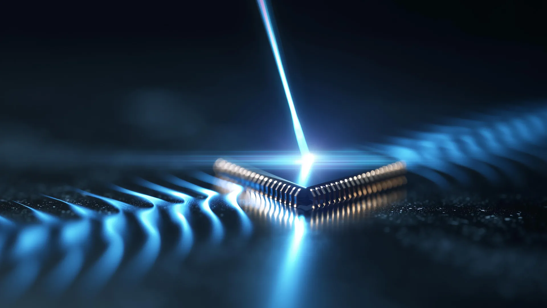
The Phonon Laser: A New way to Generate Waves
The research team has pioneered a novel method for generating these surface waves using a “phonon laser.” Unlike conventional lasers that emit light, this device produces controlled vibrations. “Think of it almost like the waves from an earthquake,onyl on the surface of a small chip,” describes Alexander Wendt,a graduate student at the University of Arizona and lead author of the study.
Conventional SAW systems typically require two separate chips and an external power source. This new design integrates all components onto a single chip, perhaps operating solely on battery power and achieving significantly higher frequencies.
How the Phonon Laser Works: An Analog to Optical Lasers
To grasp the functionality of this new device, it’s helpful to understand how traditional lasers operate. Diode lasers, commonly found in everyday devices, generate light by bouncing it between two tiny mirrors on a semiconductor chip. As light bounces, it interacts with energized atoms, amplifying the beam.
“Diode lasers are the cornerstone of most optical technologies becuase they can be operated with just a battery or simple voltage source, rather than needing more light to create the laser like a lot of previous kinds of lasers,” Eichenfield explains. “We wanted to make an analog of that kind of laser but for SAWs.”
The team constructed a bar-shaped device approximately half a millimeter in length, utilizing a carefully layered structure of specialized materials.
Layered Materials for Enhanced Performance
The device’s foundation is silicon, the standard material for computer chips. Above this lies a thin layer of lithium niobate, a piezoelectric material. Piezoelectric materials generate electric fields when vibrated, and conversely, vibrations can be triggered by applying an electric field. The final layer consists of an extremely thin sheet of indium gallium arsenide, a material with unique electronic properties that allows electrons to accelerate to high speeds even with weak electric fields.
This combination allows vibrations traveling along the lithium niobate surface to directly interact with the fast-moving electrons in the indium gallium arsenide, creating a powerful and efficient system.
The wave pool Effect: Amplifying Vibrations
The researchers liken the device’s operation to a wave pool. When an electric current flows through the indium gallium arsenide, surface waves are generated in the lithium niobate layer. These waves travel forward, reflect off a barrier, and return, similar to light bouncing between mirrors in a laser. each forward pass amplifies the wave, while each backward pass diminishes it.
“It loses almost 99% of its power when it’s moving backward, so we designed it to get a ample amount of gain moving forward to beat that,” Wendt clarifies. After multiple passes,the vibrations intensify until a portion escapes the device,analogous to laser light exiting its cavity.
Implications for the Future of Wireless Technology
Using this innovative approach, the team generated surface acoustic waves vibrating at approximately 1 gigahertz (billions of oscillations per second). they believe this design can be scaled to tens or even hundreds of gigahertz. Traditional SAW devices typically max out at around 4 gigahertz, making this new system significantly faster.
Eichenfield anticipates that this advancement will lead to smaller, more powerful, and energy-efficient wireless devices. Currently, smartphones rely on multiple chips to repeatedly convert radio waves into SAWs and back again during tasks like sending messages, making calls, or browsing the internet. The researchers aim to streamline this process by integrating all signal processing onto a single chip using surface acoustic waves.
“This phonon laser was the last domino standing that we needed to knock down,” Eichenfield concludes. “Now we can literally make every component that you need for a radio on one chip using the same kind of technology.”
Publication Date: 2026/01/24 05:12:14