
SK Hynix Invests $13 Billion in Advanced Chip Packaging to Meet AI Demand
Published: 2026/01/19 08:04:21
SK Hynix, a leading global memory chip manufacturer, is substantially expanding its chip packaging capabilities with a massive $13 billion (19 trillion won) investment in a new facility in Cheongju, South Korea. This strategic move underscores the growing demand for advanced chip packaging, particularly driven by the explosive growth of artificial intelligence (AI) applications and the need for high-bandwidth memory (HBM).
The Rise of Chip Packaging and Why It Matters
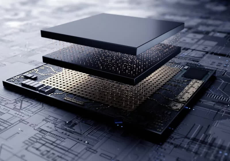
For years, the focus in the semiconductor industry has been on shrinking transistors and improving chip design. However, as those advancements become increasingly challenging and expensive, chip packaging has emerged as a critical differentiator. Chip packaging is the process of encapsulating and connecting the silicon die to the rest of the system. Advanced packaging techniques allow for greater density, faster speeds, and improved power efficiency – all crucial for AI workloads.
traditional chip packaging methods are reaching their limits. Advanced techniques like fan-out wafer-level packaging (FOWLP) and 2.5D/3D stacking are now essential for integrating multiple chips and maximizing performance.HBM, a type of high-performance RAM used in AI accelerators and GPUs, relies heavily on advanced packaging to achieve its impressive bandwidth and low latency. Without advancements in packaging, the progress in chip design would be severely hampered.
SK Hynix’s New Facility: P&T7
The new facility, dubbed P&T7 (Package & Test 7), will be dedicated to advanced chip packaging processes. According to Korea Economic Daily, P&T7 will be completed by the end of 2027. This investment is not an isolated event; it’s part of a broader strategy to establish a global HBM packaging hub. SK Hynix already operates packaging facilities in Korea and West Lafayette, Indiana, and P&T7 will complement these existing sites.
The $13 billion investment will not only cover the construction of the facility but also the acquisition of cutting-edge equipment and the development of advanced packaging technologies. This includes technologies crucial for manufacturing next-generation HBM chips, which are vital for powering AI applications in data centers, autonomous vehicles, and consumer electronics.
HBM Demand Fuels Investment
The primary driver behind this investment is the soaring demand for HBM. AI models require massive amounts of memory bandwidth to process data efficiently. HBM provides significantly higher bandwidth than traditional DRAM, making it the preferred choice for AI accelerators. Invezz reports that SK Hynix is ramping up production to meet this growing demand.
The competition in the HBM market is fierce, with companies like Samsung and Micron also investing heavily in advanced packaging. SK Hynix’s move is a clear signal that it intends to remain a leading player in this critical market segment. The company’s ability to secure a stable supply of advanced packaging capacity will be crucial for meeting the demands of its customers, including major AI chip designers like NVIDIA and AMD.
Impact on the Semiconductor Industry
SK Hynix’s investment is expected to have a ripple effect throughout the semiconductor industry. It will create new jobs in the Cheongju region and stimulate economic growth. More importantly, it will accelerate the development and adoption of advanced packaging technologies, benefiting the entire ecosystem.
The increased capacity for HBM packaging will also help to alleviate supply constraints, potentially lowering the cost of AI hardware and making it more accessible. This could further accelerate the adoption of AI across various industries.
Looking Ahead
The demand for AI is only expected to grow in the coming years, driving continued innovation in chip design and packaging.SK Hynix’s $13 billion investment is a testament to the importance of advanced packaging in the future of computing. the company’s commitment to expanding its packaging capabilities will position it well to capitalize on the opportunities presented by the AI revolution. As AI models become more complex and data-intensive, the need for high-performance memory and advanced packaging will only intensify, making SK Hynix’s strategic investment a crucial step towards meeting the challenges and opportunities ahead.