Revolutionary High-Temperature Memory Chip Breakthrough
The 200°C thermal ceiling hasn’t been a suggestion; it’s been a hard physical law for silicon-based architectures. For decades, pushing electronics past this limit meant immediate failure, forcing engineers into a constant battle of heat sinks and active cooling. A new prototype from the University of Southern California suggests that wall has finally been breached.
The Tech TL;DR:
- Thermal Threshold: Operates reliably at 700°C (1,300°F), effectively eliminating thermal throttling in extreme environments.
- Architecture: A nanoscale memristor “sandwich” utilizing tungsten, hafnium oxide ceramic, and graphene.
- Performance: 1.5V operating voltage, tens of nanoseconds speed, and over one billion switching cycles.
Standard memory chips are essentially fragile. When heat spikes, the atomic structure of the semiconductor degrades, leading to data corruption or total hardware collapse. This is why space probes and deep-earth drilling equipment require massive, heavy cooling systems that eat into the payload budget. The research led by Joshua Yang, published March 26, 2026, in Science, shifts the paradigm by replacing standard silicon components with materials that thrive where others melt.
The Material Stack: Why Tungsten and Graphene?
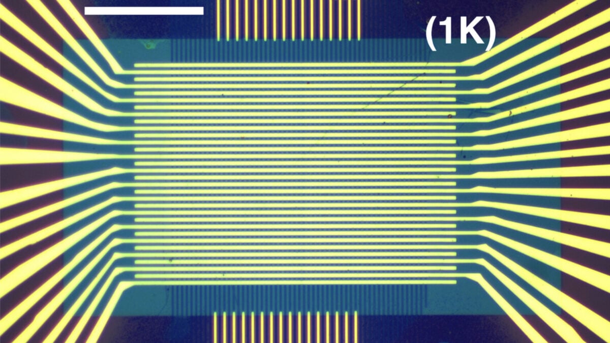
The device is a memristor—a component capable of both storing data and performing computing operations at the same location. This eliminates the traditional von Neumann bottleneck where data must travel between the CPU and RAM, a process that generates significant heat. The USC team achieved this stability through a specific three-layer material stack.
| Layer | Material | Technical Role | Key Property |
|---|---|---|---|
| Top Electrode | Tungsten | Electrical Contact | Highest melting point of any element (3,422°C) |
| Middle Filling | Hafnium Oxide | Dielectric/Storage | High-temperature ceramic stability |
| Bottom Electrode | Graphene | Conductive Base | One-atom-thick carbon sheet; extreme thermal resistance |
This combination allows the chip to hold data for over 50 hours at 700°C without needing a refresh cycle. Because the testing equipment capped at 700°C, the actual physical limit of the device remains unknown, suggesting the ceiling is even higher. For enterprise IT and industrial sectors, Which means the ability to deploy edge computing directly into combustion chambers or planetary surfaces without the latency overhead of remote data transmission.
“You may call it a revolution. It is the best high-temperature memory ever demonstrated.”
Integrating this into a production environment requires more than just a memory chip. As noted in recent reports, a complete computing system requires high-temperature logic circuits to match this memory. Until those are standardized, we are looking at a hybrid architecture. Companies managing these transitions often rely on industrial hardware consultants to bridge the gap between lab prototypes and field-ready SoC (System on a Chip) integration.
Implementation: Simulating Memristive State Transitions
From a developer perspective, interacting with a memristor differs from standard NAND or DRAM. You aren’t just flipping a bit; you are modulating resistance. Although the physical hardware is proprietary, the logic for managing state transitions in a high-temperature memristive array can be modeled via a simple resistance-voltage relationship.
# Simplified Memristor State Simulation # Based on USC prototype specs: 1.5V operating voltage def update_memristor_state(voltage, current_resistance): # Threshold for state switching V_THRESHOLD = 1.5 if voltage >= V_THRESHOLD: # 'Set' operation: Decrease resistance to store a '1' new_resistance = current_resistance * 0.85 elif voltage <= -V_THRESHOLD: # 'Reset' operation: Increase resistance to store a '0' new_resistance = current_resistance * 1.15 else: # Maintain state (Retention phase) new_resistance = current_resistance return new_resistance # Example: Processing a switching cycle at 700C initial_r = 1000 # Ohms state_1 = update_memristor_state(1.5, initial_r) state_0 = update_memristor_state(-1.5, state_1) print(f"Initial: {initial_r} | Set: {state_1} | Reset: {state_0}") The Bottleneck: Beyond the Memory Chip
The hardware is impressive, but the deployment reality is more complex. A memory chip that survives 700°C is useless if the bus connecting it to the processor melts at 200°C. We are currently seeing a massive gap in high-temperature interconnects and logic gates. This creates a significant triage point for aerospace systems integrators who must now design chassis that can handle extreme gradients—where the memory is scorching but the surrounding logic is shielded.
the transition to memristive computing will require a complete overhaul of how we handle data persistence. Traditional file systems are not optimized for components that perform computing and storage in the same cell. This will likely lead to a new class of NPU (Neural Processing Unit) architectures that can handle AI inference directly on the memory chip, drastically reducing the energy cost of LLM deployments in the field.
As we move toward integrating these components into actual hardware pushes, the focus shifts from "can it survive" to "can it scale." The billion-cycle durability is a start, but enterprise-grade reliability requires trillions of cycles. Those tasked with auditing these new hardware deployments should engage specialized hardware auditors to ensure that the atomic-level stability claimed in the Science paper holds up under real-world vibrational and pressure stresses.
The trajectory is clear: we are moving away from the silicon-only era. By leveraging graphene and tungsten, we aren't just improving the current stack; we are building a new one. The goal is no longer just managing heat—it's utilizing it.
Disclaimer: The technical analyses and security protocols detailed in this article are for informational purposes only. Always consult with certified IT and cybersecurity professionals before altering enterprise networks or handling sensitive data.