NVIDIA Expands NVLink Fusion With NVHBM for Next-Generation AI Infrastructure
NVIDIA NVLink Fusion Expands With NVHBM Custom High-Bandwidth Memory
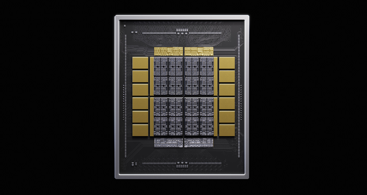
As trillion-parameter AI models and complex agentic workloads push data centers to their absolute limits, NVIDIA has expanded its NVLink Fusion architecture with NVHBM, a custom high-bandwidth memory technology designed to decouple memory controllers from custom accelerators. Announced on August 27, 2026, according to the official NVIDIA AI Blog, the platform addresses the primary bottleneck in modern AI factories: data movement between high-bandwidth memory and custom processors.
The Tech TL;DR:
- Architecture Shift: NVHBM integrates NVIDIA’s custom memory controller directly into the 3D HBM stack rather than wasting valuable silicon area on the XPU compute die.
- Performance Metrics: Per official NVIDIA specifications, the architecture delivers up to 30% greater memory bandwidth and 15% lower HBM power consumption while freeing up to 25% more area on XPU compute dies compared with standard HBM4E.
- First Adoption: Amazon’s Annapurna Labs is the initial partner collaborating on the technology, slated to support NVLink Fusion with next-generation Trainium4 chips.
Resolving the Silicon Real Estate and Bandwidth Bottleneck
Traditional HBM configurations force hardware architects to squeeze memory controllers directly onto the accelerator die. This design choice sacrifices valuable silicon acreage that could otherwise house raw compute engines. According to technical documentation published on developer.nvidia.com, moving the controller into the HBM base die changes the physical constraints of accelerator design. By reclaiming up to 25% of compute die area, hyperscalers can dedicate more transistor budget to specialized execution units and larger tensor cores.
Data starvation remains the silent killer of cluster efficiency during large-scale training and inference phases. Training algorithms, KV cache reads, and activation lookups require massive, continuous memory throughput. According to benchmarks provided in NVIDIA’s technical overview, NVHBM yields up to 30% more memory bandwidth per stack than standard HBM4E while cutting HBM power consumption by 15%. For enterprise engineering teams managing massive GPU clusters, those power savings compound quickly across thousands of server nodes.
To implement custom accelerators leveraging this tier of performance, infrastructure planners frequently rely on vetted hardware integration partners and specialized software engineering consultancies to validate custom ASIC packages before data center deployment.
Rack-Scale Integration and the AWS Annapurna Labs Collaboration
Hardware interoperability has historically plagued proprietary accelerator programs. To mitigate integration friction, NVIDIA is establishing a standardized NVHBM implementation across multiple leading memory suppliers. This multi-vendor validation pipeline drastically lowers the engineering overhead required to qualify memory components, as reported by aistart.ai.
Amazon’s Annapurna Labs is the pioneer adopter working directly with NVIDIA on the NVHBM initiative. According to statements from Nafea Bshara, vice president of Annapurna Labs at Amazon, published in the foundational NVIDIA release, Annapurna will support NVLink Fusion starting with its upcoming Trainium4 chips. This architecture allows custom Amazon silicon and NVIDIA GPUs to interoperate seamlessly within a shared rack-scale framework.
# Example: Validating XPU Telemetry over NVLink Fabric
nvidia-smi topo -m
nvlink-fusion-cli --status --verify-stack --hbm-tier=nvhbm
Through NVLink Fusion, ecosystem partners gain modular access to NVLink chiplets, NVLink-C2C interconnects, and MGX rack systems. Organizations looking to integrate these heterogeneous nodes into existing enterprise environments often partner with certified datacenter infrastructure specialists to manage complex network topology and containerized orchestration layers.
Architectural Advantages of the NVHBM Standard
Deploying advanced scaling techniques like expert parallelism (EP) and WideEP demands deterministic, high-speed synchronization across distributed compute domains. When different model experts reside on discrete physical accelerators, data must cross the scale-up fabric instantly. By keeping local compute engines continuously fed with data via NVHBM, the fabric minimizes latency spikes during multi-step reasoning tasks.
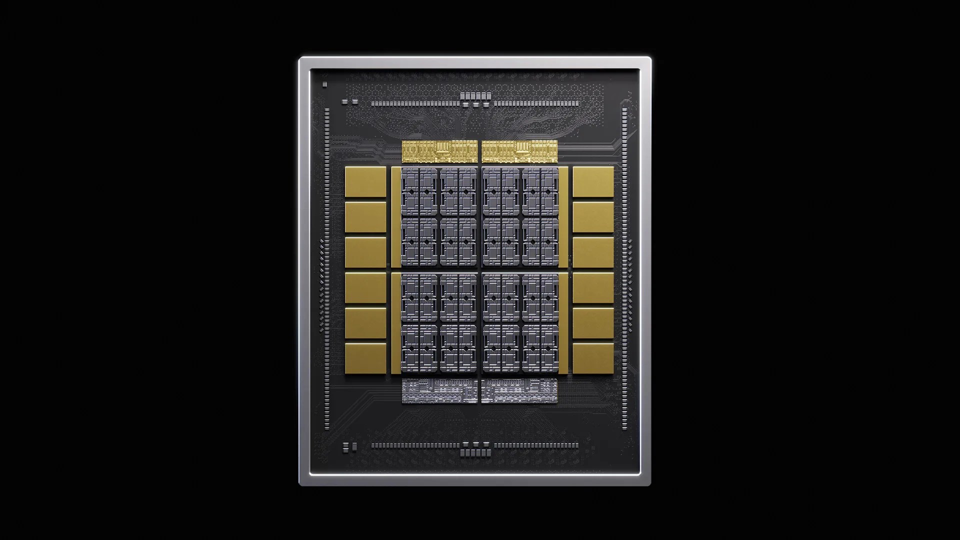
- Bandwidth: Up to 30% increase in memory bandwidth compared to standard HBM4e equivalents.
- Area Efficiency: Up to 25% more silicon area freed on the XPU die for expanded accelerator capabilities.
- Power Efficiency: Up to 15% reduction in power draw at the HBM stack level.
By standardizing these base dies across suppliers, NVIDIA aims to shorten development cycles for hyperscale cloud providers building semi-custom AI silicon.
The Editorial Kicker: The Trajectory of Semi-Custom AI Infrastructure
As the AI hardware market matures past generic GPU deployments, the competitive advantage is shifting toward deeply co-designed systems where compute, memory, and networking operate as a single unified entity. NVIDIA’s push toward an open, vertically integrated NVLink Fusion ecosystem signals that closed architectures are giving way to semi-custom modular design. For enterprise CTOs charting infrastructure roadmaps over the next five years, engineering agility will depend entirely on how cleanly their custom silicon integrates into standardized, high-bandwidth rack architectures.