Nagoya University Develops GZO Nanosheets to Enhance Compact Camera Resolution
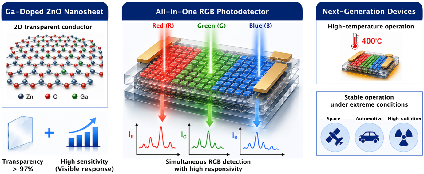
Researchers at Nagoya University in Japan have developed gallium-doped zinc oxide (GZO) nanosheets that allow for high-resolution color imaging while significantly reducing the physical size of camera lenses. This breakthrough, detailed in recent academic findings, addresses the trade-off between device slimness and optical quality in smartphone hardware.
The primary obstacle in mobile photography is the “camera bump.” To capture high-quality light, lenses require a specific focal length and depth, forcing manufacturers to push lenses outward from the phone’s chassis. By utilizing GZO nanosheets, engineers can manipulate light at a near-atomic scale, potentially eliminating the need for bulky lens assemblies without sacrificing the color accuracy or clarity of the resulting image.
The Engineering Shift: Gallium-Doped Zinc Oxide
Traditional camera systems rely on thick glass or plastic elements to bend light. The Nagoya University team shifted this approach toward materials science. Gallium-doped zinc oxide is a transparent conducting oxide. When processed into ultra-thin nanosheets, these materials exhibit unique optical properties that can be tuned to filter and focus light more efficiently than bulkier materials.
This isn’t just about making a phone thinner. It is about the physics of light transmission. The GZO nanosheets maintain high transparency, meaning they don’t “muddy” the colors of the image. In a side-by-side comparison with standard thin-film materials, these nanosheets prevent the chromatic aberration—the color fringing often seen in cheap, small lenses—that usually plagues compact optics.
The integration of these sheets into a sensor array allows for a more planar architecture. Instead of a series of stacked lenses, the light is managed by a layered nanosheet system.
Global Supply Chain and the Semiconductor Pivot
The transition from traditional glass optics to GZO nanosheets will likely shift manufacturing hubs. Japan, and specifically the research corridor around Nagoya, is positioning itself as a leader in “functional materials.” This development puts pressure on traditional lens manufacturers in Germany and the U.S. to pivot toward chemical vapor deposition and nano-fabrication.
Because these nanosheets are produced via chemical processes rather than mechanical grinding and polishing of glass, the cost of scaling could drop once the infrastructure is in place. However, the initial rollout will require high-precision fabrication plants. Companies looking to integrate this technology will need to overhaul their assembly lines.
For hardware startups and electronics firms, this creates a sudden need for specialized intellectual property guidance. As these patents move from the university lab to the factory floor, firms are engaging [Intellectual Property Law Firms] to secure licensing agreements and prevent patent infringement in the crowded mobile imaging space.
Impact on Consumer Electronics and Industrial Imaging
While smartphones are the most obvious application, the implications extend to other sectors:
- Medical Endoscopy: Thinner, high-resolution cameras allow for less invasive surgical procedures.
- Drones and Aerospace: Reducing the weight of optical payloads increases flight time and payload capacity.
- Augmented Reality (AR): GZO nanosheets could enable the “smart glasses” form factor that doesn’t look like a bulky headset.
The shift toward nano-optics also introduces new challenges in device repair. Traditional lenses can sometimes be replaced or cleaned. A nanosheet-integrated sensor is essentially a single, fused unit. This increases the reliance on manufacturer-led replacements rather than third-party repairs.
As devices become more integrated and “unrepairable” by standard means, the role of certified electronics recovery and specialized repair services becomes critical. Consumers and enterprises will increasingly rely on [Electronics Repair Specialists] who possess the clean-room environments necessary to handle nano-scale components.
The Economic Ripple Effect in East Asia
Nagoya University’s research is a strategic win for Japan’s “Society 5.0” initiative, which aims to integrate high-tech solutions into all layers of society. By dominating the material science behind the next generation of cameras, Japan maintains a grip on the high-end component market, even as final assembly of phones remains largely in China and Vietnam.
This creates a dependency: the world may design the phones in California and assemble them in Shenzhen, but the “eyes” of the devices will be engineered in Nagoya. This geopolitical positioning ensures that Japanese material exporters remain central to the global tech economy.
The complexity of these new supply chains—stretching from chemical refineries to nano-fab labs to global assembly lines—requires rigorous logistical oversight. Global firms are now utilizing [Supply Chain Management Consultants] to mitigate the risks associated with sourcing rare-earth dopants like gallium, which is often subject to trade volatility.
The era of the protruding camera lens may be ending, replaced by a chemistry-driven approach to light. As the boundary between material science and photography blurs, the industry is moving toward a future where the hardware disappears, leaving only the image behind. For those navigating the legal and logistical fallout of this transition, the World Today News Directory provides a verified path to the professional services capable of managing this high-tech shift.