
Hybrid Nanocrystal Metasurface Tunes Infrared Light via Plasmon Coupling
On November 19, 2026, researchers published a study in ACS Nano describing a one-crystal-thick metasurface sheet made from randomly mixed indium oxide nanocrystals doped with 1% or 3% tin that can amplify or suppress infrared light in ways exceeding the sum of its individual parts.
Doping Levels and Light Interactions
Incoming infrared light stirs up electron waves known as plasmons on the metasurface, trapping energy on the nanocrystals and in the tiny gaps between them, phys.org reported. Depending on the frequency of the light, mismatched electron waves from neighboring 1% and 3% indium tin oxide nanocrystals either boost or suppress that energy.
The 3% tin-doped nanocrystals produce higher-energy plasmon waves than the 1% nanocrystals, according to soz6.com. Their waves intersect across the 2.5-nanometer spaces separating the particles—canceling each other out at select frequencies while strengthening one another elsewhere, much like two distinct tuning forks vibrating in water.
“We used different techniques and different theoretical backgrounds, and even though we studied them independently at first, eventually everything pointed toward a single theory and a single phenomenon,” said Yujin Park, a postdoctoral research fellow of chemical engineering at the University of Michigan and lead author of the study published in ACS Nano, which is available at DOI: 10.1021/acsnano.6c15778.
The collaborative study included researchers from the University of Texas at Austin, Oak Ridge National Laboratory, Lawrence Berkeley National Laboratory, University of Colorado Boulder, and Institució Catalana de Recerca i Estudis Avançats in Barcelona, Spain.
Spectroscopic Mapping Techniques
The research team first observed deviations from linear optical effects using a far-field infrared spectroscopy technique, which shined a light source on the material as a whole and averaged out interactions among the crystals, phys.org reported. Researchers then brought the light source closer in a near-field technique at Lawrence Berkeley National Laboratory using synchrotron infrared nanospectroscopy, or SINS.
SINS revealed that absorption varied from spot to spot depending on each particle’s immediate neighbors. An electron beam in an electron microscope at Oak Ridge National Laboratory then mapped plasmon energy patterns around individual nanocrystals with subnanometer precision.
“There are things that are invisible to light that become very obvious in the electron beam,” as noted by soz6.com, according to Delia Milliron, a senior author of the study and the James and Judith Street Professor of Chemical Engineering at U-M.
“We could readily differentiate the nanocrystals doped with 3% tin from the ones doped with 1% tin based on the way they interact with the electron beam, an interaction that’s completely invisible with light.”
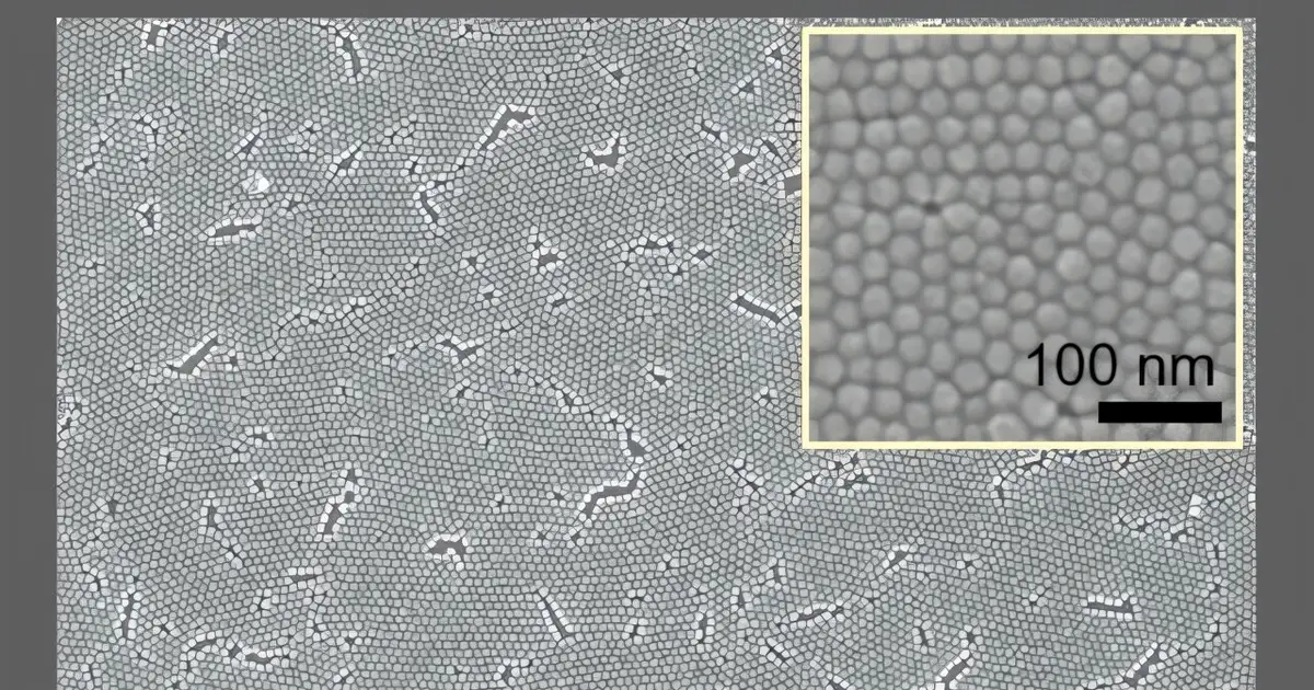
Validating Simulations Through Optical Mapping
According to sources 1 and 2, the mapping technique confirmed that the 1% and 3% ITO nanocrystals were truly randomly mixed while demonstrating how neighboring particles interact to alter light absorption. Similarly doped nanocrystals form coherently resonating subsets that underlie collective plasmon resonance hybridization, as reported in source 4.
Source 4 notes that near-field coupling between dissimilarly doped nanocrystals locally enhances fields beyond what the mixing ratio alone explains. Source 1 adds that experimental results enabled the team to build a model serving as a design tool for selecting optimal doping levels and mixing ratios.
The University of Michigan’s Department of Chemical Engineering anchors this nanophotonics advance, with professor Delia Milliron serving as the James and Judith Street Professor of Chemical Engineering at U‑M and a senior author of the 2026 ACS Nano study.
The university’s R1‑classified research enterprise, which recorded the third‑highest U.S. research expenditures in 2021, supports the interdisciplinary collaboration that combined far‑field spectroscopy, synchrotron‑based near‑field nanospectroscopy, and electron‑beam mapping to validate simulations of doped indium tin oxide nanocrystal metasurfaces.
Solution-Based Metasurface Manufacturing
Manufacturing the metasurfaces in solution sidesteps the limitations of expensive, top-down manufacturing methods like etching microscopic patterns onto a surface, helping scale up the technology.
“The experimental data from this study validate the physical picture predicted from electromagnetic simulations, paving the way for computation-guided engineering of nanocrystal-based plasmonic metasurfaces,” said Thomas Truskett, who serves as a senior author of the study alongside his role as the Vennema Professor of Chemical Engineering at U-M.
Potential applications for ultrathin nanocrystal coatings include antiglare surfaces, thermal camouflage, and materials that cool themselves using light.
“Moving forward, it’s a question of how we use near-field interactions as a further design tool for how metamaterials manipulate light, potentially converting light between frequencies or polarizing light in unusual ways,” Milliron said.